Confidential Brief — For Gary Moon, Strategic Review
Shattering the
Copper Ceiling

G2G Nano-Materials  ·  A Validated Step Beyond the Copper Ceiling

Presented by Yossi Ghinsberg  ·  Strategic Deal Architect

The 100-Year Bottleneck

A Physical Ceiling That Has
Constrained Humanity for a Century

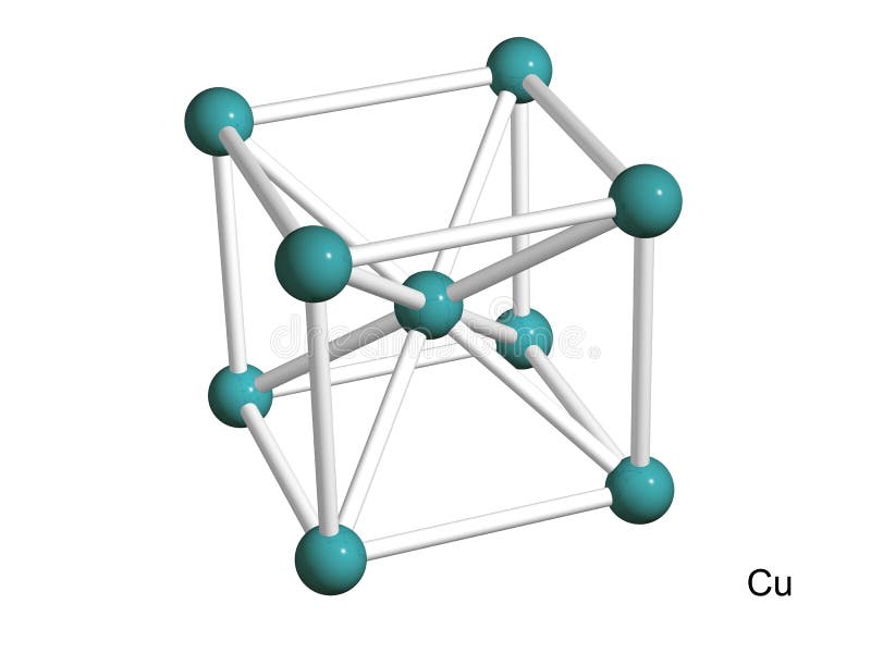
For over 100 years, engineers have accepted one immutable fact: industrial copper has a thermal conductivity ceiling of 401 W/m·K. Only silver — at 429 W/m·K — exceeds it. But silver costs ~70× more per unit weight.

This constraint has forced every engineer on the planet to compensate: larger heat sinks, heavier wiring, oversized cooling systems, lower chip densities, reduced battery efficiency. The cost — in wasted energy, materials, and performance — is measured in trillions.

401
W/m·K — The Old Copper Limit
The Only Superior Alternative
Silver — 429 W/m·K
But at 70× the cost of copper
The G2G Innovation

Copper Restructured at the Molecular Level

G2G's PureFormula™ is a proprietary organic chemistry process developed by inventor Hanan Elraz. Applied at room temperature — no industrial equipment required — it performs a surgical molecular intervention on any metal.

1
REMOVE
Residual oxygen, carbon & sulfur impurities from the crystalline lattice — eliminating electron scattering
2
RESTORE
Crystalline symmetry — re-aligning the lattice into high-purity conductivity pathways
3
GROW
Crystal structures fill vacant lattice cavities — creating better atomic connectivity throughout the material
Copper crystal lattice structure
Copper crystalline lattice — before G2G treatment
Applicable metals
Copper · Silver · Gold
Stainless Steel · Iron · Graphene
Third-Party Validated Performance

Not Theoretical. Empirically Verified.

Netzsch Instruments — Germany
Thermal Conductivity Testing
+13.78% Thermal
vs. 401 W/m·K baseline
Teldor — Certified Testing Lab
Electrical Resistance Measurement
−11% Resistance
Direct OpEx Savings
Ben-Gurion University (BGU)
Hot-Disk TPS, N=4 runs  +  SEM imaging
Independent academic
Next: Blinded Independent Replication
Neutral lab · Certified baseline · Randomized samples
In design
To make the claim airtight
🌡️
Real-World Solar Pipe Test — G2G vs. Control
52.3°C G2G  vs.  44.2°C control  →  8.1°C steady-state delta · 10.3°C peak  under identical environmental conditions
The Strategic Opportunity

Every Venture Elon Musk Controls
Runs on Copper's Limits

Venture
Copper Constraint
G2G Impact
⚡ Tesla EVs
1.8M vehicles/yr · 80–85 kg Cu/vehicle
Motor windings & battery thermal management
Lighter harnesses, extended range
🤖 Optimus Robot
28+ Cu-wound actuators · 10M/yr target
Heat generation in actuators at scale
Cooler motors, longer operation
🧠 xAI Colossus
555K GPUs · 2 GW facility · $18B infra
Cooling = 25–40% of all electricity
$200M–$500M/yr cooling savings
🚀 SpaceX / Starlink
42K satellites planned · 10× growth
Wiring, thermal pipes, rocket harnesses
Lighter satellites, lower launch mass
💾 Tesla TeraFab
2nm chip fab · 100K wafer starts/mo
Cu interconnect purity = chip yield
Better electron mobility, higher yield
The Financial Stakes

The Copper Crisis Is Live — Right Now

$6.47
Copper/lb — All-Time High
June 2026
330K
Tonnes Deficit Forecast
2026 Global Copper Market
70×
Silver's Cost Premium
Over Copper
Conductivity Performance Comparison
Standard Industrial Copper (401 W/m·K)Baseline
Pure Silver (429 W/m·K)+7% vs. Cu
G2G-Treated Copper (457+ W/m·K)+13.78% vs. Cu · Surpasses Silver
"Silver performance at copper cost — a materials arbitrage that rewrites the economics of every copper-dependent industry"
The Sleeper Hit

TeraFab: Where G2G Becomes
a Semiconductor Weapon

In January 2026, Musk announced "TeraFab" — a massive semiconductor fabrication facility near Austin targeting 100,000 wafer starts per month, scaling to 1 million, to manufacture 2nm AI chips for Tesla, SpaceX, and xAI.

His stated reason: "We either build the TeraFab or we don't have the chips." He then addressed ASML employees in June 2026 — the world's only maker of extreme ultraviolet lithography machines — confirming TeraFab as the centerpiece of his chip strategy.

At the 2nm node, copper interconnect purity is one of the most critical yield variables. G2G's molecular lattice optimization — removing oxygen, carbon & sulfur and promoting crystal growth — is precisely the process chip fabs need.

TeraFab Scale
100K → 1M
wafer starts/month target
G2G Impact on Chips
Improved electron mobility in interconnects
11% lower resistance = faster signals
Reduced electromigration = longer chip life
Higher yield = lower cost per chip
The Moat

Vertical Integration at the Molecular Level

Elon's philosophy is clear: own the supply chain. He brought battery cells in-house, built Gigafactories, replaced 70 parts with single mega-castings, and now wants a chip fab — because he hates depending on third parties.

G2G's process is not patented by design. It is held as a commercial secret — invisible to competitors, irreplicable from public disclosure.

An exclusive license or acquisition gives Musk's companies a materials advantage no competitor can access through open markets, patent databases, or supply chain strategies. This is not buying better copper — it is owning the process that makes copper better.

The Compounding Advantage
Better copper in EVs → extended range
🤖 Better copper in Optimus → cooler motors
🧠 Better copper in xAI → lower cooling costs
🚀 Better copper in SpaceX → lighter payloads
💾 Better copper in chips → higher yield
No other technology in materials science
touches all of Elon's ventures simultaneously — not as a product, but as a process upgrade to the foundational material of his entire ecosystem.
The Origin

Hanan Elraz — The Inventor

Hanan Elraz operates at the frontier of organic chemistry applied to metals. His work does not refine existing materials science, it restructures it. His process removes impurities from metal lattices at room temperature and promotes crystal growth, extending current understanding of grain-boundary chemistry at ambient conditions.

The results have been replicated across multiple metals — copper, silver, gold, stainless steel, iron, and graphene — each with similarly groundbreaking implications. He is available, motivated, and has not taken this to the open market.

The G2G Principle

"We don't just clean copper. We restructure it — restoring perfect crystalline symmetry at the atomic level, in a procedure anyone can apply at room temperature."

G2G Nano graphene product
G2G Nano-Materials — Advanced Material Science
IP Strategy — By Design

The process is not patented — it is held as a commercial secret. An exclusive partner gains a moat no competitor can reach through patent analysis or reverse engineering.

The Path

Why Peter Diamandis Is the Bridge

Peter Diamandis and Elon Musk share one of the deepest documented relationships in the technology world. Diamandis describes Musk as a "best friend" — a relationship that began when Diamandis advised Musk against starting SpaceX in 2000.

When Diamandis texted Musk proposing a climate prize, Musk pledged $100 million on the spot — which became a $157 million XPRIZE with 1,300+ competing teams. In October 2025, they appeared together live from Cape Canaveral.

This is not a cold introduction. This is one trusted friend alerting another to something that fits his worldview: a validated, physics-bending materials innovation that solves real constraints in his most ambitious projects.

The 3-Step Path
1
Peter Reviews
30-min conversation with Yossi & Hanan. No commitment — just a look.
2
Peter Introduces
Warm introduction to Elon or his materials team at Tesla/SpaceX.
3
Deal Structured
Exclusive license or acquisition — with all parties positioned appropriately.
Supporting documentation
Full third-party lab reports available upon NDA execution. Ben-Gurion University · Netzsch Germany · Teldor
The One Question

Who Gets to Know
About This First?

The technology is validated. The timing — with copper at record prices and supply deficits accelerating — is optimal. The IP is not on the open market. Not yet.

🔬
Validated
3 institutional measurements
⚗️
Scalable
Room temp · No equipment
🔒
Exclusive
Commercial secret · Not public

Yossi Ghinsberg · Strategic Deal Architect
On behalf of G2G Nano-Materials & Inventor Hanan Elraz